← Video Amplifier Circuit Board: 500W Power with C5200 and A1943 Snapklik.com : gernie mono power amplifier board power amplifier Carrier Wiring Diagram: Optimize Your HVAC System! This aircraft carrier sent its planes to attack pearl harbor but met →
If you are searching about PCB Routing Guidelines for DDR4 Memory Devices and Impedance | Blog you've came to the right web. We have 25 Pics about PCB Routing Guidelines for DDR4 Memory Devices and Impedance | Blog like pcb layout design tutorial Pcb design & layout, Pcb Layout Design Tutorial and also Step-by-step cadence PCB design tutorial - RayPCB. Here it is:
PCB Routing Guidelines For DDR4 Memory Devices And Impedance | Blog
 resources.altium.com
PCB Routing Guidelines for DDR4 Memory Devices and Impedance | Blog ...
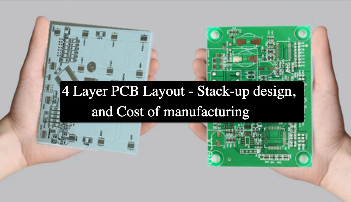
Tutorial Of 4 Layer PCB Layout, Design And Cost - AES
 absolutepcbassembly.com
Tutorial of 4 Layer PCB Layout, Design and Cost - AES
Pcb Layout Design Tutorial Pcb Design & Layout
 circuitschematics.z20.web.core.windows.net
pcb layout design tutorial Pcb design & layout
China Mobile DDR4 Lpddr4 Pcb Design And Layout Guidelines Socket
 www.chinax.com
China Mobile DDR4 Lpddr4 Pcb Design And Layout Guidelines Socket ...
Te Văd Chiriaş Strâmtoarea Bering Generate Pcb From Schematic Stres
 furnituremodern.com
Te văd chiriaş Strâmtoarea Bering generate pcb from schematic stres ...
Versal: PCB Layout Rules For 2x32 LPDDR4 Pin Efficient
Versal: PCB Layout rules for 2x32 LPDDR4 Pin Efficient
China Mobile DDR4 Lpddr4 Pcb Design And Layout Guidelines Socket
 www.chinax.com
China Mobile DDR4 Lpddr4 Pcb Design And Layout Guidelines Socket ...
Usb 2 0 Pcb Layout Guidelines - Design Talk
 design.udlvirtual.edu.pe
Usb 2 0 Pcb Layout Guidelines - Design Talk
High Current Pcb Layout Guidelines - Design Talk
 design.udlvirtual.edu.pe
High Current Pcb Layout Guidelines - Design Talk
Eagle Pcb Design Tutorial 3 Youtube - Vrogue.co
 www.vrogue.co
Eagle Pcb Design Tutorial 3 Youtube - vrogue.co
Basic Pcb Design Software
 circuitdbunerupted.z21.web.core.windows.net
Basic Pcb Design Software
Altium Pcb Layout Tutorial
 diagramlistpermalloy.z14.web.core.windows.net
Altium Pcb Layout Tutorial
Altium Designer Pcb Tutorial
 circuitwiringnosily77.z21.web.core.windows.net
Altium Designer Pcb Tutorial
Schematic To Pcb Design
 guidemanualsetter.z4.web.core.windows.net
Schematic To Pcb Design
What Are The Basic Steps Of Pcb Design - Design Talk
 design.udlvirtual.edu.pe
What Are The Basic Steps Of Pcb Design - Design Talk
Pcb Layout Design Tutorial
 manualdatacoppices.z14.web.core.windows.net
Pcb Layout Design Tutorial
Step-by-step Cadence PCB Design Tutorial - RayPCB
 www.raypcb.com
Step-by-step cadence PCB design tutorial - RayPCB
China Mobile DDR4 Lpddr4 Pcb Design And Layout Guidelines Socket
 www.chinax.com
China Mobile DDR4 Lpddr4 Pcb Design And Layout Guidelines Socket ...
PCB PRO - Tutorials, Tips, And Tricks For Using Cadence Schematic
PCB PRO - Tutorials, Tips, and Tricks for using Cadence Schematic ...
Tutorial 3 For Altium Beginners: PCB Layout
 home.fedevel.com
Tutorial 3 for Altium Beginners: PCB Layout
How To Pcb Design Tutorial At Denise Singleton Blog
 storage.googleapis.com
How To Pcb Design Tutorial at Denise Singleton blog
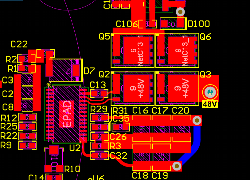
LLC Resonant Converter Design Tools And PCB Layout | Blogs | Altium
 resources.altium.com
LLC Resonant Converter Design Tools and PCB Layout | Blogs | Altium
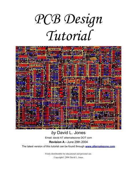
PCB Layout Tutorial By David L. Jones
 www.yumpu.com
PCB Layout Tutorial by David L. Jones
PCB Design Rules And Tips
 www.6pcb.com
PCB Design Rules and Tips
Pcb Design Using Altium
 circuitdiagrammiso.z21.web.core.windows.net
Pcb Design Using Altium
Usb 2 0 pcb layout guidelines. Eagle pcb design tutorial 3 youtube. Tutorial 3 for altium beginners: pcb layout